CodeNode Microcontrollers

CodeNode Microcontrollers is a Minecraft mod that adds mos6502 based microcontrollers to the Minecraft so you can automate your redstone contraptions with assembly code.
They act similarly to an Arduino in which you control some circuitry with code, and the CodeNode mod is a great way to expierment and learn about computing by offering a new fun way to intereact with Redstone.
Features
- mos6502 based microcontrollers
- Assembly programming
- IDE Screen with a code editor, cpu status, and memory viewer
Getting Started
Head over to the Getting Started page to help you get started using the microcontrollers in the mod!
Getting Started
One of the simplest ways to get started is by using the Nano microcontroller. It is the cheapest microcontroller that has the least amount of memory and pins. It is a great way to learn the basics of assembly programming and how to interact with the GPIO pins.
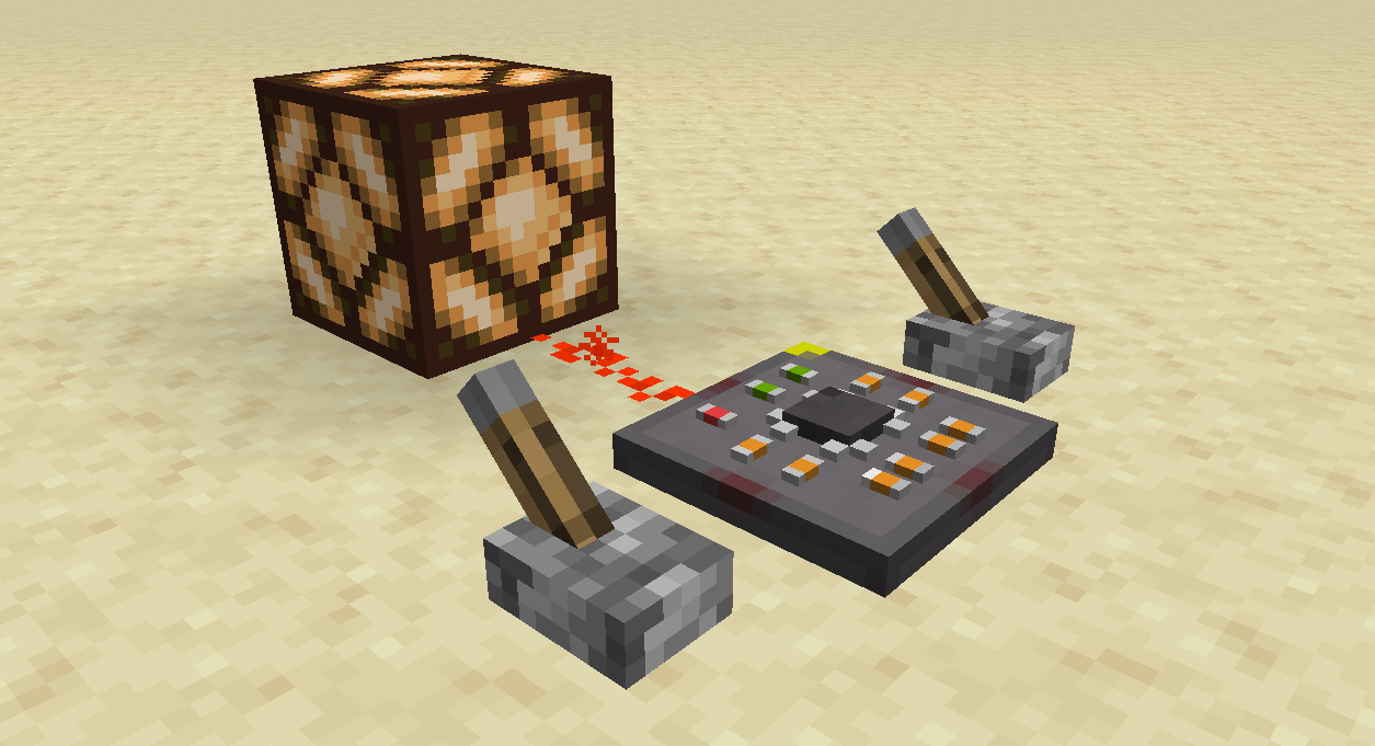
We are going to make this microcontroller act as a simple logic OR gate. We will use the GPIO pins to read the input and output the result to another pin.
Acquire the Nano
To get started, you need to acquire the Nano microcontroller. Currently, the only way to get it is by using the /give command. You can use the following command to get the Nano:

Boilerplate Code
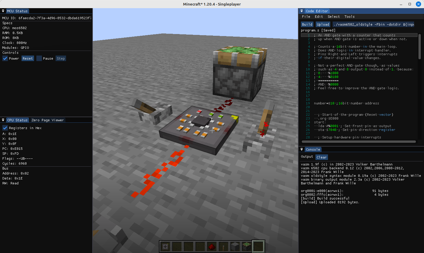
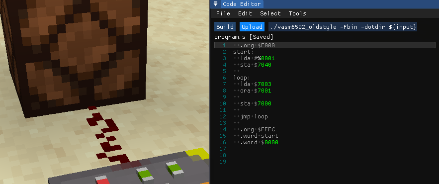
Right click the Nano to open the IDE Screen. On the top right, you'll find the Code Editor window. This is where you can write your assembly code.
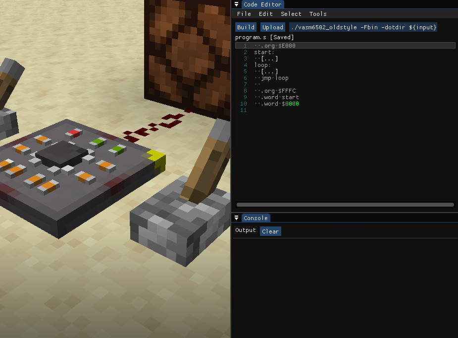
You'll need to write boilerplate code to setup the processor's vectors and starting location. It will also include the start and loop sections of the code.
  .org $E000 ; Start of the program memory
start:
  [...]
loop:
  [...]
  jmp loop ; Jump back to the loop

  .org $FFFC ; Near the end of the program memory
  .word start ; Reset vector
  .word $0000 ; Interrupt vector (not used)
Setup the GPIO Pins
We are going to use the front pin as the output of the OR gate. The left and right pins will be the inputs.
For this case, we need to set the pins' directions by setting the GPIODIR0 register. We write the binary value 0001 to the register to set the front pin as an output and the rest as inputs.
start:
  lda #%0001
  sta $7040 ; GPIODIR0
Quick Syntax Explanation
We are using the old_style syntax for the assembly code, and it is used commonly for the 6502. Here are some quick syntax explanations:
- The
#symbol is used to denote an immediate value. This means that the value is a constant and not a memory address. - The
%symbol is used to denote a binary value. This means that the value is in binary format. - The
$symbol is used to denote a hexadecimal value. This means that the value is in hexadecimal format.
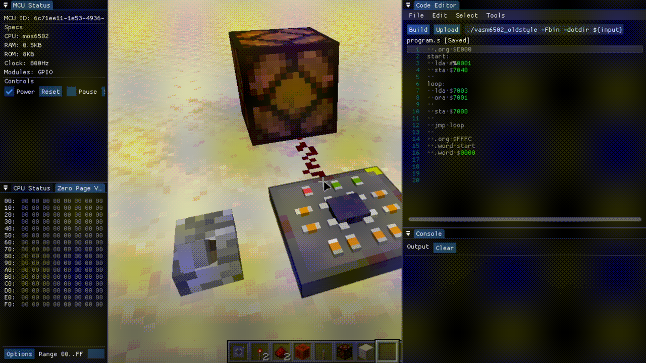
Read the Input Pins
Before we can perform the OR operation, we need to read the input pins. Since the ORA instruction uses the A register and a value in memory as inputs, we will just need to store one of the pin's value in the A register (left pin in this case).
loop:
  lda $7003 ; GPIOPV3 (Left pin)

  jmp loop
We will do this in the loop section of the code so that it works continuously.
Run the ORA Operation
We will perform the OR operation between the A register and the right pin's value. The result will be stored in the A register.
loop:
  lda $7003
  ora $7001 ; OR with GPIOPV1 (Right pin)

  jmp loop
Set the Output Pin
Finally, we will write the result of the OR operation to the front pin.
loop:
  lda $7003
  ora $7001

  sta $7000 ; GPIOPV0 (Front pin)

  jmp loop
Upload the Code
Once you have written the code, you can upload it to the Nano by clicking the Upload button on the top right of the Code Editor window.
Result
As soon as you upload the code, the microcontroller will start executing the code. You can see the result by looking at the front pin. It should output the result of the OR operation between the left and right pins.
Full code:
  .org $E000 ; Start of the program memory
start:
  lda #%0001
  sta $7040 ; GPIODIR0

loop:
  lda $7003
  ora $7001

  sta $7000 ; GPIOPV0

  jmp loop ; Jump back to the loop

  .org $FFFC ; Near the end of the program memory
  .word start ; Reset vector
  .word $0000 ; Interrupt vector (not used)
Conclusion
This is a simple example of how you can use the Nano microcontroller to perform logic operations. You can experiment with different operations and modules to create more complex circuits. Have fun coding!
Next Steps
Read more about the Nano microcontroller and its modules to explore more possibilities. You can also check out the resources section for more information on the 6502 instruction set and other useful resources.
Microcontrollers
This mod has a few microcontrollers that you can use to automate your redstone contraptions. They are based on the mos6502 microcontroller, which is popular choice for hobbyists and educators.
Note: The mod is in its early stages, so there are only a few microcontrollers available. More will be added in the future.
| Microcontroller | Description | |
|---|---|---|
 | Nano | The cheapest microcontroller that has the least amount of memory and pins. |
Nano Microcontroller
The cheapest microcontroller that has the least amount of memory and pins. Great for simple projects that don't require a lot of resources.
How to Acquire
Currently, there is no crafting recipe for the Nano, and it is not accesible in the creative inventory. It can be spawned in using the /give command.
/give <your_username> cnmcu:nano
Specs
| Spec | Value | Unit | Usage |
|---|---|---|---|
| CPU | mos6502 | ||
| Clock Speed | 800 | Hz | |
| ROM | 8096 | Bytes | Program Code, Vectors, LUTs |
| RAM | 512 | Bytes | 256B ZeroPage, 256B Stack Memory |
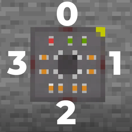
| Pins | 4 |
Pinout
Pins are numbered from 0 to 3, and they ordered in a clockwise fashion starting from the top and ending at the left. Note that the top right yellow corner of the block indicates the orientation of the pins. They are also labeled in order: front, right, back, and left.
Address Map
The Nano has a 64KB address space, with 8KB of ROM and 512 bytes of RAM.
| Address Range | Name | Uses |
|---|---|---|
0x0000 - 0x0200 | RAM | 256 bytes zero page memory | 256 byte stack |
0x7000 - 0x7070 | GPIO | Pin Control/Interrupts |
0x7100 - 0x7110 | EL | Minecraft Event Listener |
0x7200 - 0x7208 | UART | Serial Communication |
0xE000 - 0x10000 | ROM | Program Code, Vectors, LUTs |
Modules
-
GPIO - Control and read the state of the pins of a microcontroller via the processor's data bus. It has a buffer of
64bytes to store the state of every pin, but only the first four are used by the pin drivers. -
EL - Provides a simple way to listen for Minecraft events to execute code in response.
-
UART - Serial communication module that allows the microcontroller to send and receive data to and from other devices.
Registers
Head to this page to see the registers available in the Nano microcontroller: Nano Registers
GPIO
The GPIO module controls and reads the state of the pins of a microcontroller via the processor's data bus. This module can control up to 64 pins, and a single pin can be configured to be an INPUT or an OUTPUT.
Additionally, when a pin is an INPUT, it is capable of triggering interrupts to execute code when a certain event is detected.
Terms
- Pin Value: A register containing an input or output Redstone signal strength level.
- Code: Refering to the processor (the 6502) that is executing machine code.
- Byte Pin: A byte containing a pin value.
- Pin Driver: A device that samples or sends a Redstone signal from a physical pin.
- Zero Based: Arrays that begins indexing elements from 0.
Working With Digital and Analog Signals
Each pin is capable to recieve/send analog and digital signals. This is possible due to the fact that Redstone signals have 16 levels from 0 to 15, so the code of the microcontroller can interperet them as either.
Analog
When a pin is designated to read or write analog signals, pin values can be interperted as such (0x0 -> 0xF).
Digital
When a pin is designated to read or write digital signals, there can only be two possible states, 0 or 1. So in this case, when a pin value is 0, then the digital value is 0. Otherwise, any pin value greater than 0 is a digital 1 such as 0xC.
Generally when writing a digital 1, it is recommended to write 0xF (15) to the pin value so it can output the strongest possible signal to represent it.
Working With Interrupts
This module is capable of triggering interrupts to the processor; this applies to all pins. This is a great alternative to polling the pin's state because the processor will not have to spend clock cycles continously fetching updates from this module.
Furthermore, interrupts are used in timing critical situations since the processor will be notified of a certain event immediatley, and polling, on the other hand, may not be able to tend to an event at all (especially if the poll rate is slow).
For this module, the IRQ line of the processor is held LOW until all interrupt flags in the GPIOIFL are cleared.
Pin Values Buffer (GPIOPV)
The module has a buffer of 64 bytes to store the state of every pin (not all channels may be used). Each byte corresponds to a single pin.
Since Redstone signals has a range of 0 through 15, only the first four bits of a byte pin are used by the pin drivers. In essence, pin values should not increment over 15 as it will cause an undesired effect of the pin value to overflow to 0 even though the pin value is not 0. To further clarify, when pin values are represented as hexidecimal values, the second digit is ignored (ex. 0xC8 will just be 0x8).
This buffer can be read from the processor, but a byte pin can only be written to if the corresponding pin is an OUTPUT. If the pin is an INPUT, only the pin driver will write to the byte pin.
Pin Direction Buffer (GPIODIR)
The module has a buffer of 8 bytes to store the direction of every pin (INPUT or OUTPUT) which has 64 directional flags, one for each pin.
When accessing this buffer, it is to be treated as an array of bits, so, for example, the 35th bit is on the 4th byte, 3rd bit. You can use the following formulas to get the indexes for a bit (array are zero-based):
- Byte index:
floor( n / 8 ) - Bit index:
n % 8
When the nth bit is a 0, the nth pin is an INPUT. When the nth bit is a 1, the nth pin is an OUTPUT. Note that when a pin is an INPUT, the corresponding byte pin cannot be written to by the processor, and it can only be written to by the pin driver.
This buffer can be read from and written to by the processor.
Interrupt Type Buffer (GPIOINT)
The module has a buffer of 32 bytes to store the interrupt type of every pin.
Every pin has an interrupt flag the size of 4 bits (a nibble). When accessing this buffer, it is to be treated as an array of nibbles, so, for example, the 17th nibble is on the 8th byte, 1st nibble. You can use the following formulas to get the indexes for a nibble (array are zero-based):
- Byte index:
floor( n / 2 ) - Nibble index:
n % 2
The interrupt type of a pin can be one of the following:
0x0:NO_INTERRUPT- Pin does not trigger an interrupt0x1:LOW- Pin triggers an interrupt while it isLOW0x2:HIGH- Pin triggers an interrupt while it isHIGH0x3:RISING- Pin triggers an interrupt when it transitions fromLOWtoHIGH0x4:FALLING- Pin triggers an interrupt when it transitions fromHIGHtoLOW0x5:CHANGE- Pin triggers an interrupt when it transitions fromLOWtoHIGHorHIGHtoLOW0x6:ANALOG_CHANGE- Pin triggers an interrupt when the pin value changes0x7:ANALOG_RISING- Pin triggers an interrupt when the pin value increases0x8:ANALOG_FALLING- Pin triggers an interrupt when the pin value decreases0x9:NO_CHANGE- Pin triggers an interrupt when the pin value does not change
By default, all pins have NO_INTERRUPT set, but any illegal flags may cause undefined behavior.
This buffer can be read from and written to by the processor.
Interrupt Flags Buffer (GPIOIFL)
The module has a buffer of 8 bytes to store the interrupt flags of every pin (NOT_TRIGGERED or TRIGGERED).
When accessing this buffer, it is to be treated as an array of bits, so this is similar to the GPIODIR buffer. You can use those formulas to get the indexes for a bit.
When the nth bit is a 0, the nth pin has not triggered an interrupt. When the nth bit is a 1, the nth pin has triggered an interrupt. Note that when a pin has triggered an interrupt, the code must clear the flag to 0 to allow the pin to trigger another interrupt. The processor can clear the flag by writing a 1 to the nth bit.
Note that the processor can only clear the flag, and the pin driver can only set the flag.
Potential Pitfalls
If any of the following interrupt types are set, the processor will not be able to clear the flag while the interrupt is still active:
LOWHIGH
For example, if the interrupt type is set to LOW, the flag cannot be cleared until the pin is not LOW.
For interrupts to work, a pin must be an INPUT, and the interrupt type must be set to a value other than NO_INTERRUPT. However, if the pin is an OUTPUT, then no matter what interrupt type is set, the flag will be locked to 0 and will never trigger an interrupt.
Registers
Register addresses depends on every microcontroller, so you have to refer to their respective summaries to know where the GPIO registers are located. Find the register summaries here.
EL (Event Listener)
The EL module provides a simple way to listen for Minecraft events and execute code in response. You may be able to poll for events in a loop, or you may enable interrupts for certain events.
Note: Currently, the only use for this module is to listen for game ticks, but in the future, it will be expanded to include other events.
Events
This module supports up to 64 different events. The following events are currently implemented:
| Index | Event Name | Description |
|---|---|---|
| 0 | Game Tick | Fires every game tick. |
Working with Interrupts
To enable an interrupt for an event, you must set the corresponding bit in the Interrupt Control Buffer (ELICL).
This module loops through each event and checks if interrupts are enabled for it. If it is enabled and the corresponding flag is set in the Interrupt Flags Buffer, the interrupt is triggered. If there are unhandled interrupts, the IRQ line of the processor will remain held LOW until all interrupts are handled (flags are cleared).
For example, if the Game Tick event interrupt is enabled and the flag is set, the module will trigger an interrupt.
Interrupt Control Buffer (ELICL)
This module has a buffer of 8 bytes to store interrupt control data. Each bit in this buffer corresponds to an event (not all are used). If the bit is set, the interrupt for that event is enabled. If the bit is cleared, the interrupt for that event is disabled.
When accessing this buffer, it is to be treated as an array of bits. The first byte of the buffer corresponds to the first 8 events, the second byte corresponds to the next 8 events, and so on. You can use the following formulas to get the indecies for a bit (array is zero-based):
- Byte index:
floor( n / 8 ) - Bit index:
n % 8
This buffer can be read from and written to by the processor.
Interrupt Flags Buffer (ELIFL)
This module has a buffer of 8 bytes to store interrupt flags. Each bit in this buffer corresponds to an event (not all are used). If the bit is set, the interrupt for that event has occurred. If the bit is cleared, the interrupt for that event has not occurred.
Simliar to the ELICL buffer, this buffer is to be treated as an array of bits. You can use the same formulas to get the indecies for a bit.
This buffer can be read from and written to by the processor. Writing a 1 to a bit will clear the corresponding flag.
Note: These flags are set regardless of whether the interrupt is enabled or not. This allows code to poll for events if desired.
Registers
Register addresses depends on every microcontroller, so you have to refer to their respective summaries to know where the EL registers are located. Find the register summaries here.
UART (Serial Communication)
The UART module is a serial communication module that allows the microcontroller to communicate with other devices using the Universal Asynchronous Receiver/Transmitter (UART) protocol. It is capable of sending up to 20 bits per second using vanilla Redstone wire.
This module is designed similarly to the ACIA 6551 chip, which is a serial communication chip used in the Commodore 64 computer.
Terms
- Baud Rate: The number of bits per second that the module can transmit or receive.
- Data Frame: A data frame is a sequence of bits that contains the data to be transmitted or received. It consists of a start bit, data bits, an optional parity bit, and 1 or 2 stop bits.
- Start Bit: The start bit is used to indicate the beginning of a data frame. The start bit is always
1. - Data Bits: The data bits are the bits that contain the data to be transmitted or received. The number of data bits can be set to
1or8bits. - Parity Bit: The parity bit is used to check the integrity of the data. The parity bit can be set to
EVENorODDparity. - Stop Bit: The stop bit is used to indicate the end of a data frame. The stop bit is always
0.
Working Principle
This module has two data registers, UARTTXD and UARTRXD, which are used to transmit and receive data respectively. The module also has UARTCTL and UARTCMD registers to configure serial communication.
Upon writing data to the UARTTXD register, the module will start transmitting the data to the connected device. If it is recieving data, the module will store the data in the UARTRXD register.
If two microcontrollers are connected to each other, they must have the same configuration for the serial communication to work properly. The configuration includes the baud rate, data bits, parity, and stop bits.
Status Register (UARTSTS)
The UARTSTS register is used to check the status of the UART module. Here are the list of status flags (N/U means Not Used):
| Bit | Flag |
|---|---|
| 7 | IRQ |
| 6 | N/U |
| 5 | N/U |
| 4 | TX_BUFFER_EMPTY |
| 3 | RX_BUFFER_FULL |
| 2 | OVERRUN_ERROR |
| 1 | FRAME_ERROR |
| 0 | PARITY_ERROR |
Reading this register will return the status of the UART module and clear the IRQ, OVERRUN_ERROR, FRAME_ERROR, and PARITY_ERROR flags.
Writing to this register will trigger a software reset, which will clear all flags and reset the module's configuration to default.
Status Flags
-
IRQ- Interrupt Request: This flag is set when the UART module has finished transmitting or receiving data if their respective interrupt enable bits are set in the UARTCMD register. If this flag is set, theIRQline of the processor will be heldLOWuntil the flag is cleared. -
TX_BUFFER_EMPTY- TX Buffer Empty/Ready: This flag is set when the UARTTXD register is empty and the module is ready to transmit data. Writing data to the UARTTXD register while it is not empty will cause and overrun error. -
RX_BUFFER_FULL- RX Buffer Full: This flag is set when the UARTRXD register is full and it contains received data. -
OVERRUN_ERROR- Overrun Error: This flag is set when the UARTRXD register is full and new data is received or when the UARTTXD register is written to while it is not empty. -
FRAME_ERROR- Frame Error: This flag is set when the received data does not match the configured frame format. This is triggered specifically when the recieved stop bit is not a0. -
PARITY_ERROR- Parity Error: This flag is set when the received data does not match the configured parity bit.
Control Register (UARTCTL)
The UARTCTL register is used to configure the module's baud rate, word length, and stop bit.
| Bit 7 | Bits 6-4 | Bits 3-0 |
|---|---|---|
| STOP_BITS (1 or 2 bits) | WRDLEN (1 or 8 bits) | BAUD_RATE |
By default, it is set to 1 stop bit, 8 data bits, and a baud rate of 10. This is set every hard/software reset.
Stop Bits
Following the protocol, the stop bit is used to indicate the end of a data frame. The stop bit is always 0.
0- 1 stop bit1- 2 stop bits
Word Length
The word length is the number of bits in a data frame. The word length can be set to 1 or 8 bits. WRDLEN is a 3-bit field, so the resulting number of data bits follows this formula: WRDLEN + 1.
Baud Rate
The baud rate is the number of bits per second that the module can transmit or receive. BAUD_RATE is a 4-bit field, so the resulting baud rate follows this table:
| Value | Baud Rate |
|---|---|
0x0 | 1 |
0x1 | 2 |
0x2 | 5 |
0x3 | 10 |
0x4 | 20 |
0x5 | 50 |
0x6 | 150 |
0x7 | 300 |
0x8 | 600 |
0x9 | 1200 |
0xA | 1800 |
0xB | 2400 |
0xC | 3600 |
0xD | 4800 |
0xE | 7200 |
0xF | 9600 |
Obviously, since Minecraft only runs 20 ticks per second, the maximum baud rate is 20. Higher bit rates are planned to be supported using custom Redstone wire from the mod, and they may be added in the future.
Tip:
It is recommended to set the baud rate to
10for signal lines with repeaters and20for direct connections with Redstone wire.
Command Register (UARTCMD)
The UARTCMD register is used to configure how the module deals with received and transmitted data. Here are the list of command flags (N/U means Not Used):
| Bit | Flag |
|---|---|
| 7 | N/U |
| 6 | TX_PIN_ENABLE |
| 5 | RX_PIN_ENABLE |
| 4 | PARITY_TYPE |
| 3 | PARITY_ENABLE |
| 2 | ECHO_ENABLE |
| 1 | TX_INTERRUPT_ENABLE |
| 0 | RX_INTERRUPT_ENABLE |
Command Flags
-
TX_PIN_ENABLE- TX Pin Enable: This flag is used to enable the pin selected in register UARTTXP to transmit data. When enabled, the module will override the pin's output and transmit data. However, the pin must be anOUTPUTby setting the pin's direction using the GPIO module. -
RX_PIN_ENABLE- RX Pin Enable: This flag is used to enable the pin selected in register UARTRXP to receive data. When enabled, the module will read the pin's input to assemble incoming serial data. The pin must be anINPUTby setting the pin's direction using the GPIO module. -
PARITY_TYPE- Parity Type: This flag is used to select the type of parity bit to use. If it is set, the module will use EVEN parity, and If it is cleared, it will use ODD parity. -
PARITY_ENABLE- Parity Enable: This flag is used to enable the parity bit in the data frame. If this flag is set, the module will add a parity bit to the data frame. When receiving data, the module will check the parity bit to see if the data is correct (keep in mind that parity configuration must be the same on both devices). -
ECHO_ENABLE- Echo Enable: This flag is used to enable the echo feature. When enabled, the module will transmit the received data back throughTX. -
TX_INTERRUPT_ENABLE- TX Interrupt Enable: This flag is used to enable the interrupt request when the UARTTXD register is empty and the module is ready to transmit data. -
RX_INTERRUPT_ENABLE- RX Interrupt Enable: This flag is used to enable the interrupt request when the UARTRXD register is full and contains received data.
Transmit Data Register (UARTTXD)
The UARTTXD register is used to transmit data to the connected device. When data is written to this register, the module will start transmitting the data to the connected device.
If the TX_BUFFER_EMPTY flag is cleared while this register is written to, the module may transmit garbled data and set the OVERRUN_ERROR flag.
Receive Data Register (UARTRXD)
The UARTRXD register is used to store received data from the connected device. The instant the entire data frame is read, the RX_BUFFER_FULL status is set.
Reading this register will clear the RX_BUFFER_FULL, OVERRUN_ERROR, FRAME_ERROR, and PARITY_ERROR flag. If data is not read from this register before new data is received, the module will set the OVERRUN_ERROR flag.
Reading this register while it the RX_BUFFER_FULL flag is cleared may return garbled data.
Transmit Pin Register (UARTTXP)
The UARTTXP register is used to select the pin that will be used to transmit data. The selected pin must be an OUTPUT by setting the pin's direction using the GPIO module.
By default, the UARTTXP register is set to 0, which corresponds to the first pin in the GPIO module.
Receive Pin Register (UARTRXP)
The UARTRXP register is used to select the pin that will be used to receive data. The selected pin must be an INPUT by setting the pin's direction using the GPIO module.
By default, the UARTRXP register is set to 1, which corresponds to the second pin in the GPIO module.
Register Locations
Register addresses depends on every microcontroller, so you have to refer to their respective summaries to know where the EL registers are located. Find the register summaries here.
Register Summaries
Register addresses depends on every microcontroller, so you have to refer to their respective summaries to know where the its modules' registers are located. The following is a list of all the microcontrollers available in the mod and their register list.
| Item | Microcontroller | Modules |
|---|---|---|
 | Nano | GPIO |
Nano
Here is a summary of the registers available in the Nano microcontroller.
Modules
GPIO
In depth information about the GPIO module can be found here.
GPIOPV (Pin Value Registers)
There are 64 GPIOPV registers, each representing the value of a pin. Only the first 4 are used.
- Read: Returns the redstone signal strength of the pin.
- Write: Sets the redstone signal strength of the pin (if it is an output).
Register Table
| Address | Name | Description | Read/Write |
|---|---|---|---|
0x7000 | GPIOPV0 | Pin 0 / Front pin | R/W |
0x7001 | GPIOPV1 | Pin 1 / Right pin | R/W |
0x7002 | GPIOPV2 | Pin 2 / Back pin | R/W |
0x7003 | GPIOPV3 | Pin 3 / Left pin | R/W |
GPIODIR (Pin Direction Registers)
There are 8 GPIODIR registers, each bit representing the direction of a pin. Only 1 register is used.
- Read: Returns the value of the register.
- Write: Sets the value of the register.
Register Table
| Address | Name | Description | Read/Write |
|---|---|---|---|
0x7040 | GPIODIR0 | Pins (0 - 7) direction | R/W |
GPIODIR0 (N/U - Not Used)
| Bit 7 | 6 | 5 | 4 | 3 | 2 | 1 | 0 |
|---|---|---|---|---|---|---|---|
| N/U | N/U | N/U | N/U | Pin 3 dir | Pin 2 dir | Pin 1 dir | Pin 0 dir |
GPIOINT (Pin Interrupt Type Registers)
There are 32 GPIOINT registers, each nibble representing the interrupt type of a pin. Only the first 4 are used.
- Read: Returns the value of the register.
- Write: Sets the value of the register.
Register Table
| Address | Name | Description | Read/Write |
|---|---|---|---|
0x7048 | GPIOINT0 | Pins (0 - 1) interrupt types | R/W |
0x7049 | GPIOINT1 | Pins (2 - 3) interrupt types | R/W |
Interrupt types
| Value | Name | Description |
|---|---|---|
0x0 | NO_INTERRUPT | Disable interrupts |
0x1 | LOW | Trigger while low |
0x2 | HIGH | Trigger while high |
0x3 | RISING | On rising edge |
0x4 | FALLING | On falling edge |
0x5 | CHANGE | On digital rise or fall edge |
0x6 | ANALOG_CHANGE | On pin value change |
0x7 | ANALOG_RISING | On pin value increasing |
0x8 | ANALOG_FALLING | On pin value decreasing |
0x9 | NO_CHANGE | Trigger while no change |
GPIOINT0 (N/U - Not Used)
| Bits 7 - 4 | Bits 3 - 0 |
|---|---|
| Pin 1 interrupt type | Pin 0 interrupt type |
GPIOINT1 (N/U - Not Used)
| Bits 7 - 4 | Bits 3 - 0 |
|---|---|
| Pin 3 interrupt type | Pin 2 interrupt type |
GPIOIFL (Pin Interrupt Flag Registers)
There are 8 GPIOIFL registers, each bit representing the interrupt flag of a pin. Only 1 register is used.
If any flag is set, the IRQ line is held LOW. The flag must be cleared after the interrupt is serviced.
- Read: Returns the value of the register.
- Write: Clears bits of the register.
Register Table
| Address | Name | Description | Read/Write |
|---|---|---|---|
0x7068 | GPIOIFL0 | Pins (0 - 7) interrupt flags | R/W |
GPIOIFL0 (N/U - Not Used)
| Bit 7 | 6 | 5 | 4 | 3 | 2 | 1 | 0 |
|---|---|---|---|---|---|---|---|
| N/U | N/U | N/U | N/U | Pin 3 flag | Pin 2 flag | Pin 1 flag | Pin 0 flag |
EL (Event Listener)
In depth information about the EL module can be found here.
ELICL (Interrupt Control Buffer)
This module has a buffer of 8 bytes to store interrupt control data. Each bit in this buffer corresponds to an event (not all are used). If the bit is set, the interrupt for that event is enabled. If the bit is cleared, the interrupt for that event is disabled.
- Read: Returns the value of the register.
- Write: Sets the value of the register.
Register Table
| Address | Name | Description | Read/Write |
|---|---|---|---|
0x7100 | ELICL0 | Events (0 - 7) interrupt control | R/W |
ELICL0 (N/U - Not Used)
| Bit 7 | 6 | 5 | 4 | 3 | 2 | 1 | 0 |
|---|---|---|---|---|---|---|---|
| N/U | N/U | N/U | N/U | N/U | N/U | N/U | Game Tick |
ELIFL (Interrupt Flags Buffer)
This module has a buffer of 8 bytes to store interrupt flags. Each bit in this buffer corresponds to an event (not all are used). If the bit is set, the interrupt for that event has occurred. If the bit is cleared, the interrupt for that event has not occurred.
- Read: Returns the value of the register.
- Write: Clears bits of the register.
Register Table
| Address | Name | Description | Read/Write |
|---|---|---|---|
0x7108 | ELIFL0 | Events (0 - 7) interrupt flags | R/W |
ELIFL0 (N/U - Not Used)
| Bit 7 | 6 | 5 | 4 | 3 | 2 | 1 | 0 |
|---|---|---|---|---|---|---|---|
| N/U | N/U | N/U | N/U | N/U | N/U | N/U | Game Tick |
UART
In depth information about the UART module can be found here.
There are 7 registers in the UART module.
Register Table
| Address | Name | Description | Read/Write |
|---|---|---|---|
0x7200 | UARTSTS | Status | R |
0x7201 | UARTCTL | Control | R/W |
0x7202 | UARTCMD | Command | R/W |
0x7203 | UARTTXD | Transmit Data | R/W |
0x7204 | UARTRXD | Receive Data | R |
0x7205 | UARTTXP | Transmit Pin | R/W |
0x7206 | UARTRXP | Receive Pin | R/W |
0x7207 | UART_ | Internal | R |
UARTSTS (Status Register)
The UARTSTS register is used to check the status of the UART module. Here are the list of status flags (N/U means Not Used):
| Bit | Flag |
|---|---|
| 7 | IRQ |
| 6 | N/U |
| 5 | N/U |
| 4 | TX_BUFFER_EMPTY |
| 3 | RX_BUFFER_FULL |
| 2 | OVERRUN_ERROR |
| 1 | FRAME_ERROR |
| 0 | PARITY_ERROR |
Reading this register will return the status of the UART module and clear the IRQ, OVERRUN_ERROR, FRAME_ERROR, and PARITY_ERROR flags.
Writing to this register will trigger a software reset, which will clear all flags and reset the module's configuration to default.
UARTCTL (Control Register)
The UARTCTL register is used to configure the module's baud rate, word length, and stop bit.
| Bit 7 | Bits 6-4 | Bits 3-0 |
|---|---|---|
| STOP_BITS (1 or 2 bits) | WRDLEN (1 or 8 bits) | BAUD_RATE |
Stop Bits
| Value | Bits |
|---|---|
0 | 1 stop bit |
1 | 2 stop bits |
Word Length
The word length is the number of bits in a data frame. The word length can be set to 1 or 8 bits. WRDLEN is a 3-bit field, so the resulting number of data bits follows this formula: WRDLEN + 1.
Baud Rate
The baud rate is the number of bits per second that the module can transmit or receive. BAUD_RATE is a 4-bit field, so the resulting baud rate follows this table:
| Value | Baud Rate |
|---|---|
0x0 | 1 |
0x1 | 2 |
0x2 | 5 |
0x3 | 10 |
0x4 | 20 |
0x5 | 50 |
0x6 | 150 |
0x7 | 300 |
0x8 | 600 |
0x9 | 1200 |
0xA | 1800 |
0xB | 2400 |
0xC | 3600 |
0xD | 4800 |
0xE | 7200 |
0xF | 9600 |
By default, it is set to 1 stop bit, 8 data bits, and a baud rate of 10. This is set every hard/software reset.
UARTCMD (Command Register)
The UARTCMD register is used to configure how the module deals with received and transmitted data. Here are the list of command flags (N/U means Not Used):
| Bit | Flag |
|---|---|
| 7 | N/U |
| 6 | TX_PIN_ENABLE |
| 5 | RX_PIN_ENABLE |
| 4 | PARITY_TYPE |
| 3 | PARITY_ENABLE |
| 2 | ECHO_ENABLE |
| 1 | TX_INTERRUPT_ENABLE |
| 0 | RX_INTERRUPT_ENABLE |
UARTTXD (Transmit Data Register)
The UARTTXD register is used to write data to the UART module. Writing to this register will transmit the data.
UARTRXD (Receive Data Register)
The UARTRXD register is used to read data from the UART module. Reading this register will return the received data.
UARTTXP (Transmit Pin Register)
The UARTTXP register is used to set the transmit pin. Writing to this register will set the transmit pin.
UARTRXP (Receive Pin Register)
The UARTRXP register is used to set the receive pin. Writing to this register will set the receive pin.
UART_ (Internal Register)
The UART_ register is an internal register that is not meant to be used by the user. Reading from this register will return undisclosed data.
Resources
Here are some resources that may be useful when working with the Redstone microcontroller.
mos6502 Instruction Set
While this documentation site does contain the list of opcodes and their descriptions, these sites may be useful for a more in-depth look at the 6502 instruction set.
Ben Eater's 6502 Computer Video Series
This is a great series that goes over the 6502 microprocessor and how to build a computer with it. It is a great resource to learn about the 6502 and how everything is working under the hood.
This is were this inspiration for this mod came from!
The 8-Bit Guy's Video Essay on the 6502
This is a great video essay that goes over the history of the 6502 and shows how it powered a whole generation of computers.